Synopsis
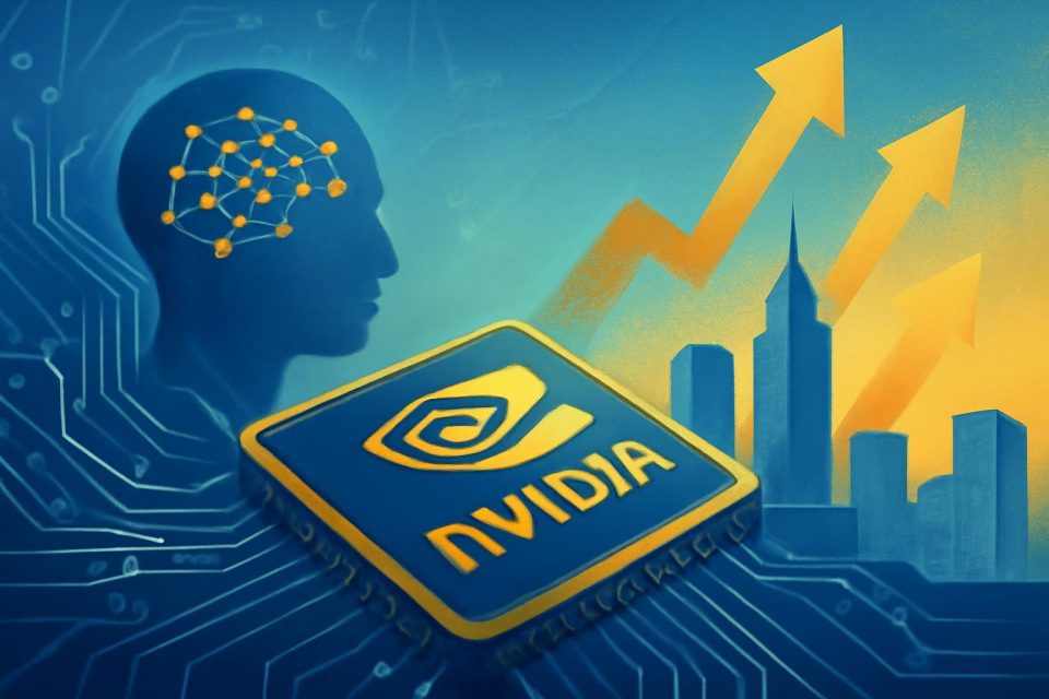
Odisha is emerging as a significant player in advanced sectors like electronics and semiconductors with the inauguration of India's first 3D glass substrate packaging facility. This Rs 1,943 crore project, set up by 3D Glass Solutions Inc., aims to bolster India's semiconductor value chain and support future technologies like AI and high-performance computing.The facility is being set up by USA-based 3D Glass Solutions Inc. (3DGS), through its wholly owned Indian subsidiary Heterogenous Integration Packaging Solutions Pvt. Ltd. (HIPSPL). It will manufacture cutting-edge glass substrate technologies, a first of its kind in the country. The minister said such advanced packaging will play a key role in the future of semiconductors, especially in areas like artificial intelligence and high-performance computing.
"It is indeed a historic day today for Odisha," he said. "It's very important for Odisha to have a world-class, latest technology industry here. Odisha is now becoming an IT hub (and) an electronics manufacturing hub. For years, industries like mining, metal and power have existed in the state, but now it is taking steps towards the high-tech industry."
The IT minister said two semiconductor projects have already been approved for Odisha under the India Semiconductor Mission, while three more electronics and semiconductor-related proposals are in the pipeline. “Discussions are also underway with major global companies, including Intel for future investments in the state. I have requested (Intel CEO) Lip-Bu Tan that he sees Odisha as a top priority,” he said.
The facility is designed as a vertically integrated operation combining substrate manufacturing, assembly and advanced packaging within a single site, which is distinct from conventional OSAT models. It aims to deploy innovations such as glass interposers and 3D heterogeneous integration modules—key components for next-generation computing systems. These technologies are expected to support sectors including artificial intelligence, photonics and high-performance computing.
"PM Modi's vision is to create a semiconductor ecosystem that not only has the technology but also has the scale," Babu Mandava, chairman and CEO of 3D Glass Solutions said. "In manufacturing technology is important but scale is equally important. We are a small and important piece of the puzzle to start this process."
He said the vision of the company was to build the highest capacity fab and that this was the first step in that direction.
HIPSPL which is backed by US tech majors including chip maker Intel whose CEO Lip-Bu Tan joined the groundbreaking ceremony virtually. Tan, on his part, highlighted the factors that worked in Odisha's favour for the project.
"Odisha offers surplus power, abundant and reliable water resources, and a growing base of skilled talent. Together, these create a strong and sustainable foundation for advanced manufacturing,” he said in a statement.
This project is one of two semiconductor-related investments cleared earlier by the Centre for Odisha in 2025. The other, led by SiCSem Private Limited, will manufacture silicon carbide-based devices with applications across defence, electric mobility, rail infrastructure and renewable energy systems. Together, these initiatives are part of a wider national effort to expand domestic semiconductor capabilities.
Odisha chief minister Mohan Charan Majhi spoke of the project being a 'defining step' in its semiconductor journey while reiterating his pitch for the state. He called it a historic milestone that positions Odisha at the forefront of global electronics manufacturing and artificial intelligence.
"For the global semiconductor industry, our message is clear: We have power, we have talent, we have infrastructure, we have resolve," he said. "If you are looking for the right place to build the technologies of tomorrow- Odisha is your destination...This is not merely an industrial investment; it is a declaration of where the technologies of tomorrow will be built."